

|
THE POWER VAULT |

|
|
PREMIUM DISCRETE CIRCUITRY |
THE TOPOLOGY
The DMA-260 utilizes FET and high speed bipolar transistors in a dense, fully balanced topology to achieve high-current launch and ultra-fast settling capability. RF (radio frequency) design techniques are employed to achieve a DC coupled power band with intrinsic bandwidth to almost 5 MHz.
Input Stage. The shielded input stage utilizes a balanced, double cascode design using matched differential pairs of J-FET's. The cascode design derives its own ground reference and produces extremely high levels of isolation from the preamplifier and between the stages of the DMA-260 itself.
Gain Stage. The gain stage utilizes super high frequency (RF) bipolar transistors matched in a cascode configuration to bring the circuit into the power device realm.
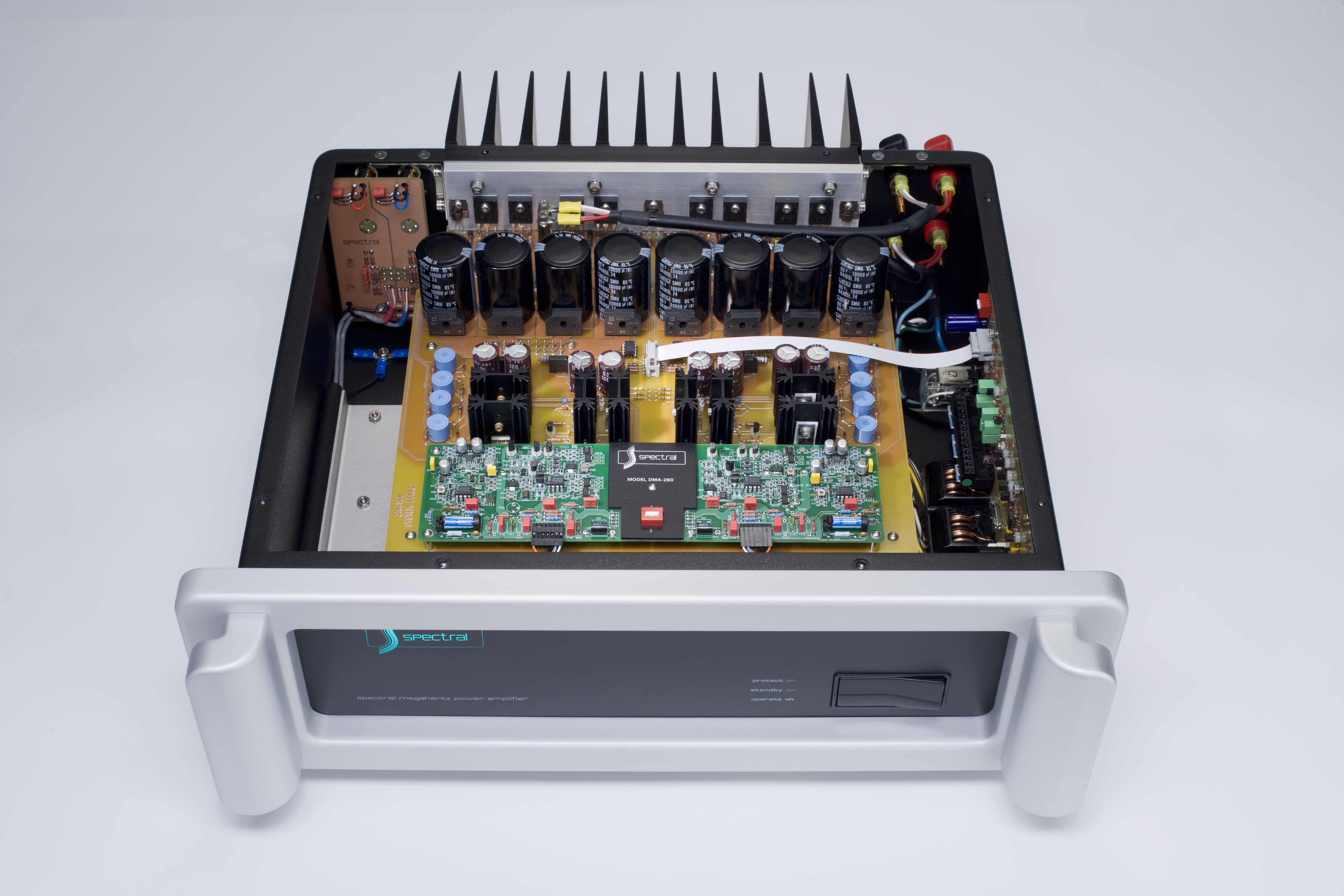
Output Stage. The power output stage utilizes push-pull drivers for the custom VMOS-FET output devices. The DC bias setting for each output device is performed individually after burn-in through Teflon trimmers. An individual high-speed switching power supply filter capacitor and full rectifier circuit is sited immediately next to each output device on the circuit board. The total energy storage capacity of this distributed power array is 256 watt seconds per channel. Each output device is also given its own individual set of high isolation transformer windings. The DMA-260's Vertical Dimensional Topology allows the signal traces to enter the output stage along the vertical, or Z axis, and all signal and current carriers are twisted into electromagnetic field-canceling knots.
|
POWER AND PRECISION IN A UNIQUE MARRIAGE |

|
|